
January 23rd 2026
We are pleased to announce the successful fabrication of an ultra-large CVD diamond heat spreader produced by MPCVD (Microwave Plasma Chemical Vapor Deposition) technology. This achievement represents a significant step forward in the industrial application of diamond materials for advanced thermal management.
CVD diamond is widely recognized as one of the most effective heat-spreading materials available today, combining extremely high thermal conductivity with electrical insulation and outstanding chemical stability. The newly developed diamond heat sink is specifically engineered to meet the increasing thermal demands of next-generation semiconductor and high-power electronic systems.
Key Technical Specifications
• Manufacturing process: MPCVD
• Material type: High-purity polycrystalline CVD diamond
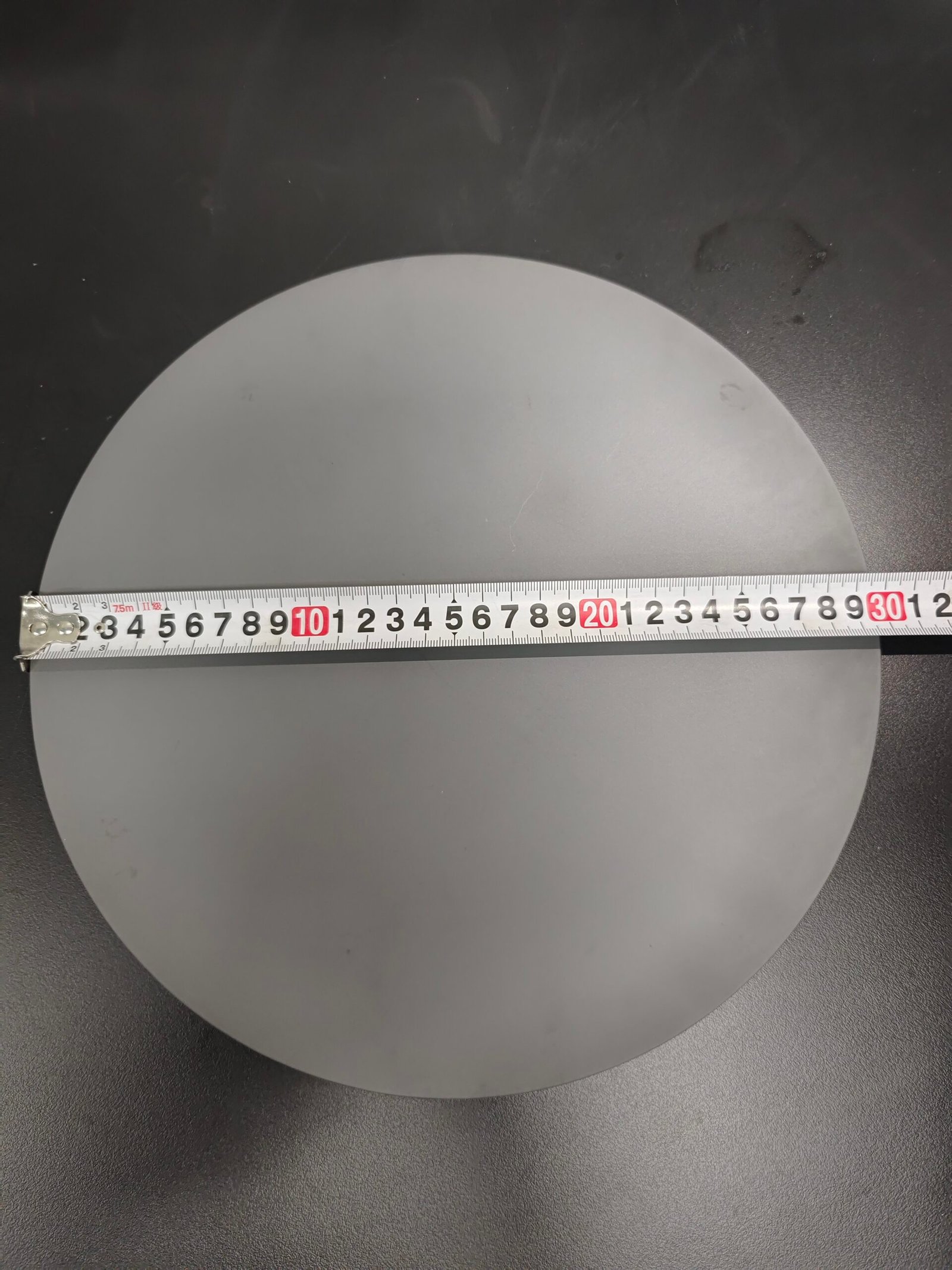
• Diameter: approximately 300 mm
• Thickness: approximately 1.0 mm
• Thermal conductivity: ≥1200 W/m·K
• Electrical properties: electrically insulating
• Surface condition: engineered for post-processing and metallization
Material Performance Advantages
The exceptionally high thermal conductivity of CVD diamond allows rapid lateral heat spreading, significantly reducing hot spots and thermal stress. Compared with conventional materials such as copper, aluminum nitride, or silicon carbide, CVD diamond offers superior heat dissipation while maintaining low thermal expansion mismatch with semiconductor devices.
Target Applications
This diamond heat spreader is well suited for:
• Power semiconductor modules (IGBT, SiC, GaN)
• RF and microwave devices
• High-power laser systems
• Advanced semiconductor packaging and thermal interface structures
By enabling higher power density, improved reliability, and longer device lifetime, MPCVD CVD diamond heat sinks are becoming a key enabling material for the future of electronics.
This development further demonstrates the growing maturity of CVD diamond technology and its critical role in next-generation thermal management solutions.