
Date: August 23, 2025
As power density surges in GaN/SiC power modules, RF front-ends, AI accelerators, and 2.5D/3D ICs, thermal bottlenecks—not transistor physics—increasingly cap performance and reliability. Chemical-vapor-deposited (CVD) diamond heat sinks and heat spreaders offer a decisive path forward for semiconductor packaging and chip encapsulation, combining ultra-high thermal conductivity, electrical insulation, and mechanical robustness that conventional materials cannot match.
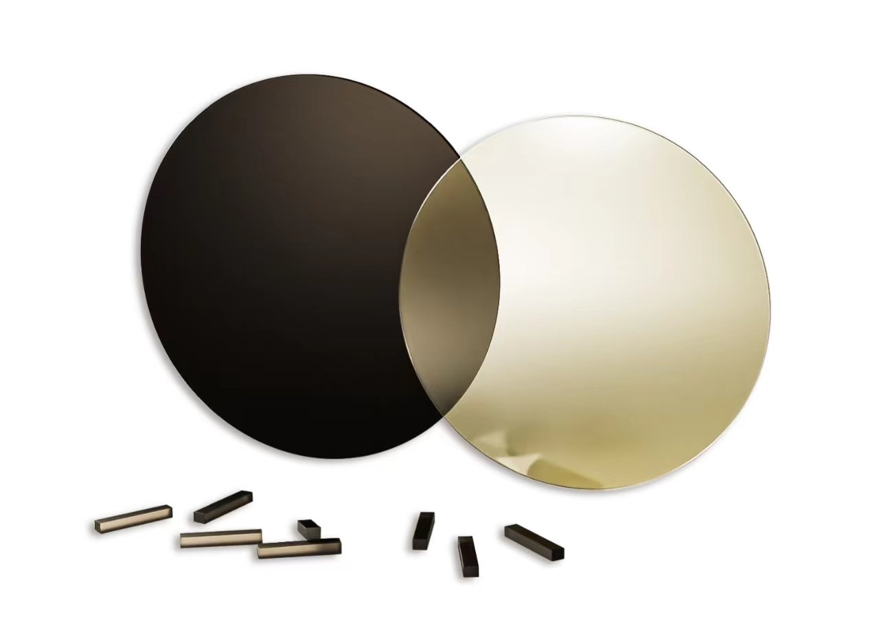
Why diamond stands apart
High-quality CVD diamond exhibits room-temperature thermal conductivity typically >2,000 W·m⁻¹·K⁻¹, while its coefficient of thermal expansion (CTE) is ~1 ppm·K⁻¹. This rare pairing enables aggressive heat spreading with minimal thermomechanical stress at die interfaces—especially valuable adjacent to GaN and SiC devices. By contrast, copper (~400 W·m⁻¹·K⁻¹), aluminum (~220), AlN (~150–200), and Si (~130–150) trail by wide margins, and most are electrically conductive or less chemically inert. Diamond’s isotropic heat transport and electrical insulation simplify stack-ups in advanced packaging without compromising creepage/clearance.
Evidence from devices and packages
In GaN HEMTs, multiple integration routes—GaN-on-diamond wafers, direct-bonded diamond submounts, and top-side polycrystalline diamond caps—consistently reduce junction temperature and enable higher RF power density. Recent work demonstrated low-temperature top-side diamond on fully fabricated AlGaN/GaN transistors, underscoring diamond’s compatibility with finished devices and the potential for drop-in thermal upgrades at the package level. Interface engineering to minimize thermal boundary resistance (TBR) remains pivotal to extracting the full benefit, and current studies map how interface quality governs long-term electrothermal degradation in GaN–diamond stacks.
At the package level, academic and industrial teams have optimized diamond-in-package concepts (e.g., diamond plates or inlays in PQFN/DFN styles) and shown measurable hotspot reductions versus identical packages without diamond. Design flows co-optimize diamond thickness, die thinning, and interface layers to minimize spreading resistance under both steady-state and transient loads—key for real workloads.

Readiness for 2.5D/3D and heterogeneous integration
Vertical heat removal is the Achilles’ heel of stacked-die systems. Recent platforms at MIT Lincoln Laboratory use purpose-built high-power test chips to evaluate cooling solutions for packaged stacks and localized hotspots—exactly the regime where diamond’s thermal conductivity and electrical insulation provide unique leverage. Industry roadmaps likewise emphasize CTE-matched, high-κ heat spreaders and better thermal interfaces as cornerstones of advanced packaging for heterogeneous integration.
Real-world deployments
Beyond laboratories, GaN-on-diamond RF power amplifiers have advanced toward commercialization in satellite communications, with reported step-ups in data rates per radio footprint owing to dramatically improved heat removal. Though application specifics vary, these efforts illustrate that diamond heat spreading is not theoretical—it is enabling compact, high-throughput radios and pointing the way for defense, 5G, and space payloads.
Practical integration and manufacturability
Modern CVD diamond heat spreaders are available in electronic/thermal grades with controlled thickness, surface finish, and metallization (e.g., Ti/Pt/Au, W, AuSn-ready) to support soldering, diffusion bonding, or transient-liquid-phase attach. Robust metallization stacks and careful surface preparation reduce TBR and improve reliability under thermal cycling. As volumes rise and wafer-scale processing matures, cost and variability continue to decline, making diamond increasingly accessible for high-value assemblies in power electronics and high-performance computing.
Outlook: from premium option to essential enabler
The trajectory is clear. With localized heat fluxes already pushing >1 kW·cm⁻² in hotspots for RF and AI accelerators, and with tighter form-factor constraints in chiplet and 3D IC packages, diamond’s combination of ultra-high thermal conductivity, electrical insulation, low CTE, and chemical stability is uniquely suited to safeguard performance and lifetime. Expect broader adoption of:
- Diamond caps/inlays in GaN RF PAs and power modules;
- Diamond lids or submounts co-designed with TIMs and vapor-chamber lids;
- Selective diamond interposers for 2.5D/3D stacks where electrical isolation is mandatory;
- Standardized thermal design kits (TDKs) that model diamond accurately in package/board co-simulation.
As the ecosystem converges on system-level thermal codesign, CVD diamond heat sinks will evolve from niche “hero” parts to standard building blocks for reliable, high-power, high-density electronics.